A Nanosecond Pulse Generator based on the Reconfigurable Phase-Locked Loop (PLL) Module in Field Programmable Gate Arrays (FPGAs)
Members
Zhang Xing Jian A0226453H, Zhang Jian Ran A0226340R, Chua Rui Ming A0155387U
Motivation
Field Programmable Gate Arrays (FPGAs) offer both the advantage of Programmable Logic Devices (PLDs) and Application Specific Integrated Circuits (ASICs) because it possesses the functional flexibility without the simplicity of the former and the functional complexity without the inflexibility of the latter1 (Maxfield, 2008). Furthermore, they are cheap and easy to implement which enables small groups to meet their hardware and software needs1 (Maxfield, 2008). As a result, FPGAs represent a useful option to the production of narrow pulses which finds its role in a myriad of scientific applications2 (Zhu & Wang, 2015). In our context, the generation of narrow pulses is of particular interest in the field of integrated photonics, for example, in the carving of pump light into short pulses for Spontaneous Four-Wave Mixing (SFWM) in silicon microring resonators3 (Ma, 2020). The use of FPGAs to produce narrow pulses provides us with a compact and adjustable pulse generator compatible with integrated photonics technology.
FPGA Specifications
Product
Our FPGA is the "DE0-Nano Development and Education Board" from Terasic (vendor)4 (Terasic Technologies, n.d.). The FPGA utilises Intel Altera's Cyclone IV family, specifically, the Cyclone IV E variant5 (Intel, n.d.). It measures 49 x 75.2mm.
Architecture
Some features of the make-up of our FPGA includes:
- 22,320 Logic Elements
- 594 Embedded memory (Kbits)
- 66 Embedded 18 x 18 multipliers
- 4 General-purpose PLLs
- 53 Maximum FPGA I/O pins
Its memory features 32MB Synchronous Dynamic Random-Access Memory (SDRAM), 2Kb I2C Electrically Erasable Programmable Read-Only Memories (EEPROM), and it has an on-board 50MHz clock oscillator4 (Terasic Technologies, n.d.).
Preview
The top and bottom view of the FPGA is featured below respectively4 (Terasic Technologies, n.d.).


Phase-Locked Loop (PLL) Module
The PLL is the key component to our nanosecond pulse generator and would thus be elaborated upon in the following section. A PLL is a feedback control system that locks on the output signal of an oscillator to an input signal by monitoring and maintaining a phase between them. In Altera's FPGAs, the structure of the PLL is as follows7 (Intel, 2018):
- A "Phase Frequency Detector" is used to compare the feedback signal with the input signal for any errors between them
- A "Charge Pump" is used to convert said error, which manifests itself as an error signal, to a correction current
- A "Loop Filter" is used to produce a correction signal from the correction current which is subsequently used to regulate the oscillation frequency of the "Voltage Control Oscillator"
- The signal is then fed through the "Feedback Counter" back to the "Phase Frequency Detector" to complete the loop
Architecture of Altera's FPGA's PLL7 (Intel, 2018)
_IP_Core_User_Guide.png)
Methods
Since the PLL is reconfigurable, the phase, frequency and bandwidth of the PLL output signal may be adjusted in real-time. Logic operations may be executed on two signals produced by the PLL to "carve" out the difference between the two signals into a desired narrow pulse. In Zhu & Wang's paper (2015), they utilised the steps and logic operations to obtain such a pulse:
- The production of two clock signals A and B of the same frequency, with a phase shift.
- The implementation of an A OR B operation to produce clock signal C
- The implementation of a D = C XOR A operation to carve out the difference between the two signals to produce the narrow pulse
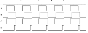

In our case, our method deviates from that of Zhu & Wang by implementing a two-step procedure to carve out the pulse. This was achieved simply by skipping the A OR B operation. There are two reasons for our choice: Firstly, this simplifies the problem. Secondly, this way, we obtain two pulses for every set of clock signals- At the front-end and tail-end of the first and second clock signals respectively:
- The production of two clock signals A and B of the same frequency, with a phase shift.
- The implementation of an C = B XOR A operation to produce the narrow pulses

For the uninitiated, the OR and XOR logic operation can be described by the truth tables and illustrated by the pulsed operations below as referenced from Electronics Hub8,9 (Electronics Hub, 2017)


Results
FPGA Top Design
The FPGA Top Design summarises the outcome of our code behind the design of our FPGA. To characterise the performance of our FPGA, we measured the pulses produced by our FPGA (see below). We recall that one of the strengths of the FPGA lies in its adjustability; By adjusting the phase difference between the clock signals or the frequency of the clock signals we can obtain different performances (in terms of different pulse width and frequencies) of our FPGA. Hence, we characterised the performance of our FPGA as a function of the Phase Difference and as a function of Clock Frequency.
Pulses as a function of Phase Difference
Pulses as a function of Frequency
The clock frequency may be adjusted in integer multiples of the clock oscillator (refer to FPGA Architecture).
Summary Table
Application
References
[1] Maxfield, C. (2008). Fpgas: Instant access. In FPGAs: Instant access (1st ed., pp. 1-12). Burlington, MA: Newnes/Elsevier.
[2] Zhu, Y., & Wang, L. (2015). Design and implementation of nanosecond Pulse generator based ON RECONFIGURATION PLL in FPGA. Proceedings of the 2015 International Conference on Electronic Science and Automation Control. doi:10.2991/esac-15.2015.78
[3] Ma, C. (2020). High-Quality Photon Pair Generation in Silicon Photonic Microring and Its Applications. UC San Diego. ProQuest ID: Ma_ucsd_0033D_19192. Merritt ID: ark:/13030/m5sf83ns. Retrieved from https://escholarship.org/uc/item/7ws930nj
[4] Terasic Technologies. (n.d.). All FPGA boards - Cyclone IV - DE0-Nano development and Education Board. Retrieved March 23, 2021, from https://www.terasic.com.tw/cgi-bin/page/archive.pl?Language=English&CategoryNo=139&No=593&PartNo=3#section
[5] Intel. (n.d.). Cyclone® IV Fpgas devices - Intel® FPGA. Retrieved March 23, 2021, from https://www.intel.sg/content/www/xa/en/products/programmable/fpga/cyclone-iv.html
[6] Intel. (2020). Intel® Quartus® Prime Software Suite. The Intuitive High-Performance Design Environment. Retrieved March 22, 2021, from https://www.intel.com/content/www/us/en/software/programmable/quartus-prime/overview.html
[7] Intel. (2018, December 20). Altera phase-locked Loop (ALTERA PLL) ip core user guide. Retrieved March 23, 2021, from https://www.intel.com/content/www/us/en/programmable/documentation/mcn1401782837027.html
[8] Electronics Hub. (2017, December 24). Digital logic or gate. Retrieved March 29, 2021, from https://www.electronicshub.org/digital-logic-or-gate/#OR_Gate
[9] Electronics Hub. (2017, December 24). Exclusive or Gate(XOR-Gate). Retrieved March 29, 2021, from https://www.electronicshub.org/exclusive-or-gatexor-gate/#XOR_Gate